
Applications by Industry
Advanced Manufacturing & Semiconductor
High-temperature masking, UV-release dicing tape, plating protection, and clean room converted adhesive components for semiconductor and advanced manufacturing processes.
Application Snapshot
High-temperature masking for process protection
UV-release dicing tape for wafer handling
Clean room converted adhesive components
Process Integrity, Contamination Control, and Clean Removal in Semiconductor Manufacturing
Semiconductor and advanced manufacturing processes place extreme demands on adhesive tapes and films. Process tapes must withstand aggressive chemical environments, high temperatures, and plasma exposure without adhesive bleed, residue, or substrate contamination. UV-release dicing tapes must maintain wafer fixation during sawing, then release cleanly under UV exposure without die damage or adhesive residue. High-temperature masking tapes must protect metal contacts and bond pads during electroplating, etching, and soldering without leaving residue after removal. Contamination from adhesive outgassing or particulates can cause process defects, making material selection and clean-room handling critical at every stage.
ALS Tape Fit
Process Tape and Converting Solutions for Semiconductor Applications
ALS Tape supports semiconductor and advanced manufacturing buyers with process tapes for high-temperature masking, UV-release wafer processing, and electroplating protection, alongside clean room converting services for contamination-sensitive adhesive components. Functional films for insulation and protection are available in precision slit formats for automated semiconductor assembly processes.
Key Applications
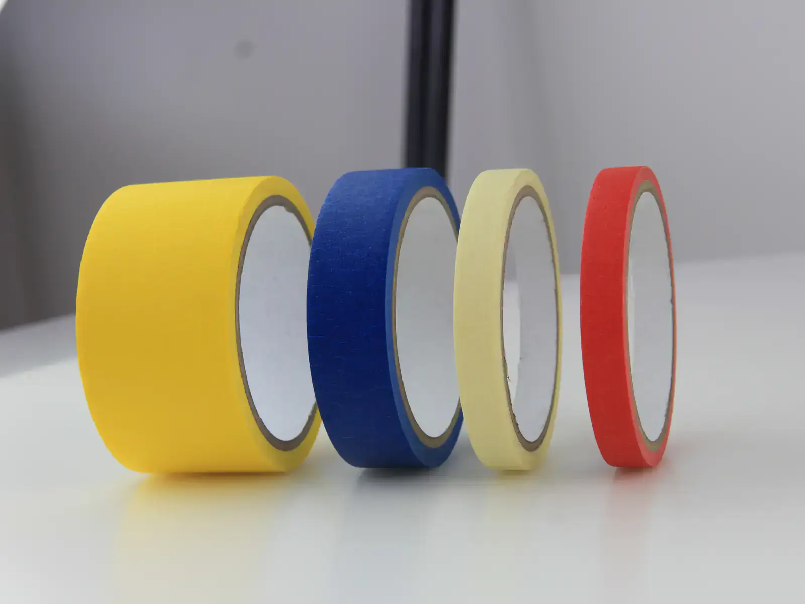
High-Temperature Masking for Process Protection
High-temperature masking tape protects bond pads, contacts, and component areas during electroplating, solder reflow, and chemical etching processes. The tape must withstand process temperatures without adhesive migration and remove cleanly without residue after the process step.
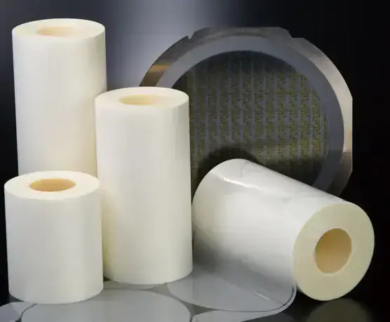
Dicing Tape and Wafer Handling
UV-release dicing tape mounts silicon, GaAs, and compound semiconductor wafers for dicing operations, maintaining fixation under cutting force and releasing cleanly when exposed to UV, enabling die pick-and-place without adhesive contamination.
Clean Room Converted Adhesive Components
Clean room die cutting and converting produces adhesive gaskets, mounting pads, and insulation components for semiconductor equipment and advanced packaging assemblies in a controlled environment that meets semiconductor cleanliness standards.
Typical Materials
Semiconductor Process Tape
UV-release dicing, high-temperature masking, and electroplating protection in semiconductor wafer and chip manufacturing
High-Temperature Masking Tape
Protection of bond pads and contacts during soldering, plating, and etching processes with clean residue-free removal
Functional Film
Precision slit insulation and protection films for semiconductor equipment assemblies and advanced packaging
Clean Room Converted Parts
Contamination-free die-cut adhesive components and gaskets for semiconductor equipment and advanced packaging applications
Recommended Products

FAQ
What is UV-release dicing tape and how does it work?
UV-release dicing tape uses an adhesive that cures and loses tack when exposed to UV light. The tape holds the wafer securely during dicing, then the UV exposure breaks the adhesive bond, allowing individual dies to be picked without adhesive residue or die damage.
What temperature rating is needed for masking tape in semiconductor processes?
Semiconductor process masking typically requires tapes rated from 150°C to 260°C depending on the process. Polyimide-backed tapes with silicone adhesive are the standard for high-temperature applications up to 260°C.
Why is clean room converting required for semiconductor adhesive components?
Particulate contamination from converting operations can cause defects in semiconductor assemblies. Clean room converting in a certified ISO Class 8 or better environment ensures that die-cut adhesive components meet the contamination control requirements of semiconductor manufacturing.
Can masking tape be precision die cut to specific chip and bond pad geometries?
Yes. Precision die cutting can produce masking tape parts to custom shapes matching specific chip outlines, bond pad arrays, and component protection zones, enabling repeatable masking without hand-cutting in production.